- 您现在的位置:买卖IC网 > Sheet目录2000 > IDT821054PQF (IDT, Integrated Device Technology Inc)IC PCM CODEC QUAD MPI 64-PQFP
42
IDT821054 QUAD PROGRAMMABLE PCM CODEC WITH MPI INTERFACE
INDUSTRIAL TEMPERATURE RANGE
8.3
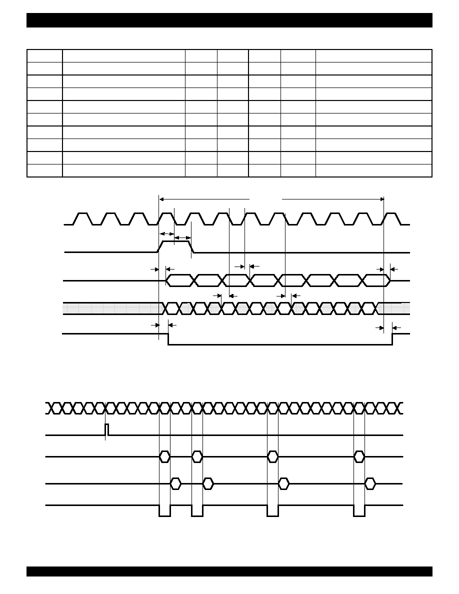
PCM INTERFACE TIMING
Figure - 11 Transmit and Receive Timing
Figure - 12 Typical Frame Sync Timing (2 MHz Operation)
Symbol
Description
Min.
Typ.
Max.
Units
Test Conditions
t21
Data enable delay time
5
70
ns
t22
Data delay time from BCLK
5
70
ns
t23
Data float delay time
5
70
ns
t24
Frame sync setup time
25
t4
50
ns
t25
Frame sync hold time
50
ns
t26
TSX1 or TSX2 enable delay time
5
80
ns
t27
TSX1 or TSX2 disable delay time
5
80
ns
t28
Receive data setup time
25
ns
t29
Receive data hold time
5
ns
1234
56781
BIT 1
BIT 2
BIT 3
BIT 4
BIT 5
BIT 6
BIT 7
BIT 8
BIT
1
BIT
2
BIT
3
BIT
4
BIT
5
BIT
6
BIT
7
BIT
8
BCLK
FS
DX1/
DX2
DR1/
DR2
t25
t24
Time Slot
t23
t22
t21
t28
t29
TSX1 /
TSX2
t26
t27
Note: This timing diagram only applies to the situation of receiving data on falling edges and transmitting data on rising edges.
27
28
29
30
31
01234
56789
10
11
12
13
14
15
16
17
18
19
20
21
22
23
24
25
26
X0
X1
X2
X3
R0
R1
R2
R3
Time Slot
FS
DX1/DX2
DR1/DR2
TSX1 / TSX2
发布紧急采购,3分钟左右您将得到回复。
相关PDF资料
IDT82V3001APVG8
IC PLL WAN W/SGL REF INP 56-SSOP
IDT82V3010PVG
IC PLL WAN 51/E1/OC3 DUAL 56SSOP
IDT82V3011PVG
IC PLL WAN T1/E1/OC3 SGL 56-SSOP
IDT82V3012PVG8
IC PLL WAN T1/E1/OC3 DUAL 56SSOP
IDT82V3155PVG
IC PLL WAN T1/E1/OC3 DUAL 56SSOP
IDT82V3202NLG
IC PLL WAN EBU SGL 68-VFQFPN
IDT82V3255TFG
IC PLL WAN SMC STRATUM 3 64-TQFP
IDT82V3280APFG
IC PLL WAN SE STRATUM 2 100TQFP
相关代理商/技术参数
IDT821054PQFG
功能描述:IC PCM CODEC QUAD MPI 64-PQFP RoHS:是 类别:集成电路 (IC) >> 接口 - 编解码器 系列:- 标准包装:2,500 系列:- 类型:立体声音频 数据接口:串行 分辨率(位):18 b ADC / DAC 数量:2 / 2 三角积分调变:是 S/N 比,标准 ADC / DAC (db):81.5 / 88 动态范围,标准 ADC / DAC (db):82 / 87.5 电压 - 电源,模拟:2.6 V ~ 3.3 V 电压 - 电源,数字:1.7 V ~ 3.3 V 工作温度:-40°C ~ 85°C 安装类型:表面贴装 封装/外壳:48-WFQFN 裸露焊盘 供应商设备封装:48-TQFN-EP(7x7) 包装:带卷 (TR)
IDT821064
制造商:IDT 制造商全称:Integrated Device Technology 功能描述:QUAD PROGRAMMABLE PCM CODEC WITH GCI INTERFACE
IDT821064PQF
制造商:IDT 制造商全称:Integrated Device Technology 功能描述:QUAD PROGRAMMABLE PCM CODEC WITH GCI INTERFACE
IDT821068
制造商:IDT 制造商全称:Integrated Device Technology 功能描述:OCTAL PROGRAMMABLE PCM CODEC
IDT821068PX
制造商:IDT 制造商全称:Integrated Device Technology 功能描述:OCTAL PROGRAMMABLE PCM CODEC
IDT821621
制造商:IDT 制造商全称:Integrated Device Technology 功能描述:LONG HAUL SLIC
IDT821621J
制造商:IDT 制造商全称:Integrated Device Technology 功能描述:LONG HAUL SLIC
IDT8217LP35P
制造商:Integrated Device Technology Inc 功能描述: